1. Crystal Structure and Split Anisotropy
1.1 The 2H and 1T Polymorphs: Architectural and Digital Duality
(Molybdenum Disulfide)
Molybdenum disulfide (MoS ₂) is a layered change steel dichalcogenide (TMD) with a chemical formula including one molybdenum atom sandwiched between 2 sulfur atoms in a trigonal prismatic coordination, forming covalently adhered S– Mo– S sheets.
These individual monolayers are stacked vertically and held with each other by weak van der Waals forces, making it possible for simple interlayer shear and exfoliation to atomically thin two-dimensional (2D) crystals– an architectural feature central to its diverse functional duties.
MoS ₂ exists in multiple polymorphic forms, the most thermodynamically steady being the semiconducting 2H phase (hexagonal balance), where each layer displays a direct bandgap of ~ 1.8 eV in monolayer kind that transitions to an indirect bandgap (~ 1.3 eV) wholesale, a sensation crucial for optoelectronic applications.
On the other hand, the metastable 1T stage (tetragonal balance) embraces an octahedral control and acts as a metal conductor because of electron contribution from the sulfur atoms, allowing applications in electrocatalysis and conductive composites.
Stage transitions between 2H and 1T can be generated chemically, electrochemically, or with pressure design, using a tunable platform for designing multifunctional tools.
The ability to stabilize and pattern these stages spatially within a single flake opens up paths for in-plane heterostructures with distinctive digital domain names.
1.2 Defects, Doping, and Side States
The performance of MoS ₂ in catalytic and digital applications is very sensitive to atomic-scale problems and dopants.
Intrinsic factor flaws such as sulfur jobs function as electron benefactors, increasing n-type conductivity and functioning as active websites for hydrogen evolution responses (HER) in water splitting.
Grain boundaries and line problems can either hamper charge transportation or develop local conductive pathways, depending on their atomic arrangement.
Controlled doping with shift metals (e.g., Re, Nb) or chalcogens (e.g., Se) enables fine-tuning of the band framework, carrier focus, and spin-orbit combining effects.
Notably, the edges of MoS two nanosheets, especially the metallic Mo-terminated (10– 10) sides, exhibit considerably higher catalytic task than the inert basic aircraft, motivating the style of nanostructured catalysts with maximized edge direct exposure.
( Molybdenum Disulfide)
These defect-engineered systems exhibit how atomic-level manipulation can transform a naturally occurring mineral right into a high-performance useful material.
2. Synthesis and Nanofabrication Methods
2.1 Bulk and Thin-Film Manufacturing Methods
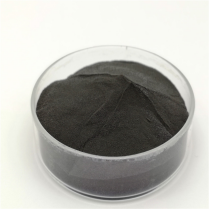
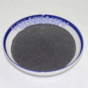
All-natural molybdenite, the mineral kind of MoS ₂, has actually been used for decades as a strong lubricating substance, however modern-day applications require high-purity, structurally controlled synthetic kinds.
Chemical vapor deposition (CVD) is the dominant technique for creating large-area, high-crystallinity monolayer and few-layer MoS two films on substrates such as SiO ₂/ Si, sapphire, or flexible polymers.
In CVD, molybdenum and sulfur precursors (e.g., MoO two and S powder) are evaporated at high temperatures (700– 1000 ° C )under controlled ambiences, allowing layer-by-layer development with tunable domain size and positioning.
Mechanical exfoliation (“scotch tape method”) stays a criteria for research-grade examples, producing ultra-clean monolayers with marginal issues, though it does not have scalability.
Liquid-phase exfoliation, including sonication or shear mixing of bulk crystals in solvents or surfactant solutions, produces colloidal dispersions of few-layer nanosheets appropriate for coatings, compounds, and ink solutions.
2.2 Heterostructure Combination and Gadget Patterning
Real potential of MoS ₂ arises when integrated right into upright or lateral heterostructures with other 2D products such as graphene, hexagonal boron nitride (h-BN), or WSe ₂.
These van der Waals heterostructures make it possible for the style of atomically precise tools, consisting of tunneling transistors, photodetectors, and light-emitting diodes (LEDs), where interlayer fee and power transfer can be engineered.
Lithographic pattern and etching methods permit the manufacture of nanoribbons, quantum dots, and field-effect transistors (FETs) with network lengths down to tens of nanometers.
Dielectric encapsulation with h-BN safeguards MoS two from ecological destruction and lowers cost scattering, dramatically enhancing carrier flexibility and tool security.
These construction developments are important for transitioning MoS two from research laboratory inquisitiveness to sensible component in next-generation nanoelectronics.
3. Practical Characteristics and Physical Mechanisms
3.1 Tribological Actions and Strong Lubrication
One of the oldest and most long-lasting applications of MoS two is as a completely dry solid lubricant in extreme settings where fluid oils stop working– such as vacuum, high temperatures, or cryogenic conditions.
The reduced interlayer shear toughness of the van der Waals void enables very easy gliding in between S– Mo– S layers, leading to a coefficient of rubbing as reduced as 0.03– 0.06 under optimal conditions.
Its efficiency is better enhanced by strong adhesion to steel surface areas and resistance to oxidation approximately ~ 350 ° C in air, past which MoO five development enhances wear.
MoS ₂ is widely made use of in aerospace systems, air pump, and weapon components, usually used as a layer using burnishing, sputtering, or composite unification into polymer matrices.
Current research studies show that humidity can degrade lubricity by enhancing interlayer attachment, prompting research study right into hydrophobic finishings or crossbreed lubricants for better ecological stability.
3.2 Digital and Optoelectronic Response
As a direct-gap semiconductor in monolayer form, MoS two shows solid light-matter communication, with absorption coefficients going beyond 10 ⁵ cm ⁻¹ and high quantum yield in photoluminescence.
This makes it suitable for ultrathin photodetectors with quick feedback times and broadband sensitivity, from noticeable to near-infrared wavelengths.
Field-effect transistors based on monolayer MoS two demonstrate on/off ratios > 10 eight and provider wheelchairs approximately 500 centimeters ²/ V · s in put on hold examples, though substrate communications typically restrict useful worths to 1– 20 centimeters ²/ V · s.
Spin-valley coupling, a consequence of strong spin-orbit interaction and busted inversion balance, allows valleytronics– an unique paradigm for information inscribing utilizing the valley degree of freedom in energy room.
These quantum sensations setting MoS ₂ as a prospect for low-power reasoning, memory, and quantum computer aspects.
4. Applications in Power, Catalysis, and Emerging Technologies
4.1 Electrocatalysis for Hydrogen Evolution Reaction (HER)
MoS two has actually emerged as a promising non-precious alternative to platinum in the hydrogen advancement reaction (HER), an essential process in water electrolysis for environment-friendly hydrogen production.
While the basal airplane is catalytically inert, side websites and sulfur vacancies exhibit near-optimal hydrogen adsorption complimentary power (ΔG_H * ≈ 0), comparable to Pt.
Nanostructuring methods– such as developing up and down aligned nanosheets, defect-rich films, or doped crossbreeds with Ni or Carbon monoxide– maximize energetic website thickness and electrical conductivity.
When integrated into electrodes with conductive supports like carbon nanotubes or graphene, MoS ₂ accomplishes high present densities and long-term stability under acidic or neutral problems.
Additional enhancement is achieved by supporting the metallic 1T phase, which enhances intrinsic conductivity and exposes additional energetic sites.
4.2 Versatile Electronics, Sensors, and Quantum Gadgets
The mechanical flexibility, openness, and high surface-to-volume ratio of MoS ₂ make it excellent for versatile and wearable electronic devices.
Transistors, logic circuits, and memory tools have actually been demonstrated on plastic substrates, making it possible for bendable displays, wellness monitors, and IoT sensing units.
MoS ₂-based gas sensors exhibit high sensitivity to NO ₂, NH ₃, and H TWO O as a result of bill transfer upon molecular adsorption, with feedback times in the sub-second range.
In quantum innovations, MoS ₂ hosts local excitons and trions at cryogenic temperatures, and strain-induced pseudomagnetic fields can catch providers, making it possible for single-photon emitters and quantum dots.
These growths highlight MoS two not just as a functional product yet as a system for checking out basic physics in decreased measurements.
In recap, molybdenum disulfide exhibits the convergence of classical materials science and quantum engineering.
From its ancient function as a lube to its modern-day deployment in atomically slim electronics and power systems, MoS two continues to redefine the boundaries of what is possible in nanoscale materials design.
As synthesis, characterization, and assimilation strategies development, its influence throughout science and innovation is poised to increase even additionally.
5. Distributor
TRUNNANO is a globally recognized Molybdenum Disulfide manufacturer and supplier of compounds with more than 12 years of expertise in the highest quality nanomaterials and other chemicals. The company develops a variety of powder materials and chemicals. Provide OEM service. If you need high quality Molybdenum Disulfide, please feel free to contact us. You can click on the product to contact us.
Tags: Molybdenum Disulfide, nano molybdenum disulfide, MoS2
All articles and pictures are from the Internet. If there are any copyright issues, please contact us in time to delete.
Inquiry us